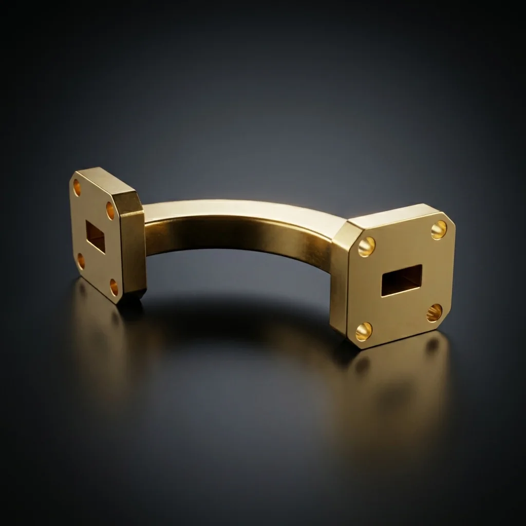
WR-03 H-Plane Bend
The WR-03 H-Plane Bend is a precision-engineered waveguide component that redirects millimeter-wave signals by 90 degrees in the broad wall (H-field) plane. It is specifically designed for the 220 - 330 GHz frequency range, serving as a critical building block in J-Band infrastructure.
H-plane bends curve along the wider dimension of the rectangular waveguide cross-section, providing horizontal signal routing without inducing higher-order modes. Operating in the extreme J-Band (220-330 GHz), WR-03 is the absolute cutting edge of commercial waveguide technology. The 0.034" x 0.017" aperture is thinner than a credit card, requiring flawless electroforming.
Key Features
H-Plane Geometry
Bend follows the broad wall (wider dimension) of the waveguide, routing signals horizontally while maintaining the narrow-wall dimension.
Low Insertion Loss
Optimized bend radius and CNC-machined interior walls ensure minimal signal degradation through the 90-degree turn.
Precision CNC Machined
Each bend is machined from a solid billet of OFHC copper, maintaining tight dimensional tolerances throughout the bend radius.
Gold-Plated Construction
Gold plating provides excellent conductivity, corrosion resistance, and consistent electrical performance over the component's service life.
J-Band Use Cases
ALMA Telescope
Sub-millimeter astronomy
THz Spectroscopy
Molecular rotational sensing
Material Science
Dielectric characterization
Medical Imaging
Non-ionizing THz scanners
More H-Plane Bends
Frequently Asked Questions
Why use an H-plane bend over an E-plane bend?+
H-plane bends are used when the signal needs to be routed horizontally across an optical table or chassis without twisting the polarization of the wave. The wider bend radius typically handles higher peak power than an E-plane bend.
What is the physical size of the WR-03 opening?+
The internal hole of a WR-03 waveguide is 0.034 inches by 0.017 inches (0.86 mm by 0.43 mm). It is so small that a standard mechanical pencil lead cannot fit inside it. Dust particles alone can severely ruin the VSWR.
Why is gold plating mandatory on WR-03?+
At 300 GHz, the skin depth of the RF signal is less than 0.1 micrometers. The signal travels exclusively on the very outer layer of atoms on the waveguide wall. Even a microscopic layer of copper oxidation will completely absorb the terahertz wave, making non-oxidizing gold plating absolutely mandatory.