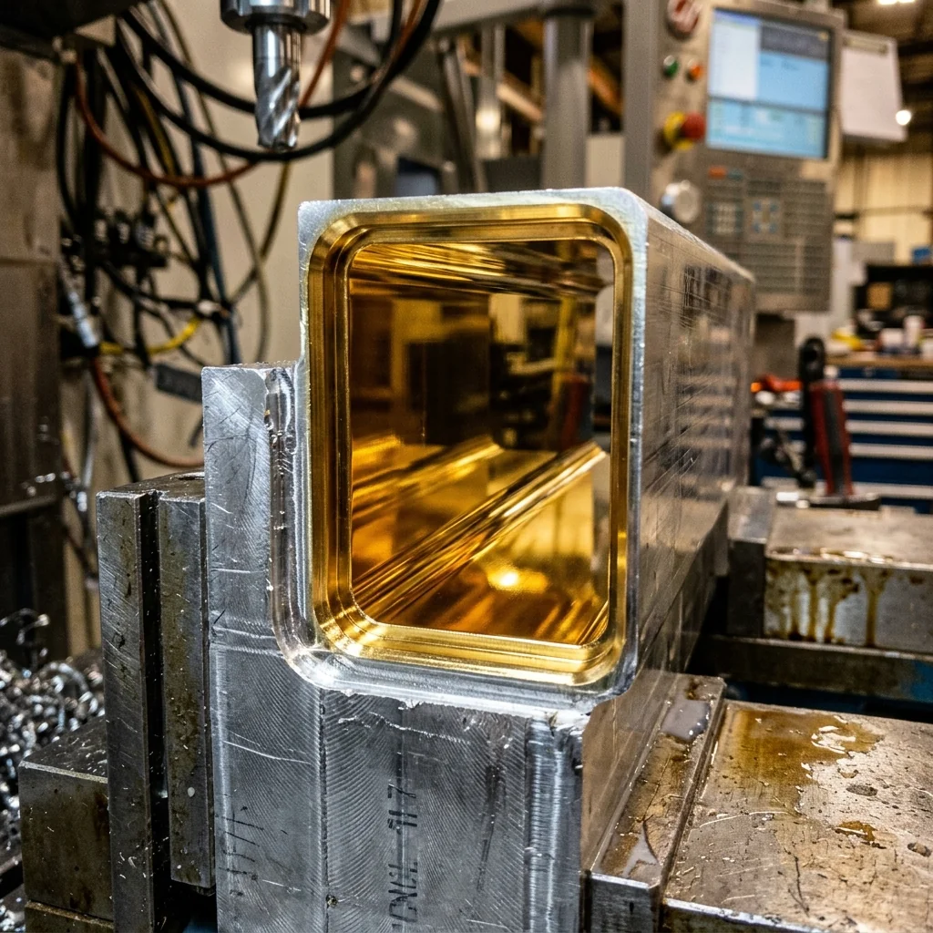
Why Surface Finish Is the Hidden Variable in Waveguide Performance
When engineers evaluate waveguide components, they focus on the specifications that appear on datasheets: frequency range, VSWR, insertion loss, and power handling. Those are the outputs. But the single manufacturing parameter that most directly controls insertion loss, and the one that is hardest to verify after the component is assembled, is the internal surface finish of the waveguide channel.
At our manufacturing facility in St. Petersburg, we have spent years refining our CNC machining processes specifically to achieve the surface roughness targets required for millimeter wave waveguide performance. The relationship between surface roughness and conductor loss is governed by fundamental electromagnetic physics, and at Ka-band and above, there is no room for compromise.
Skin Depth: Where the Current Actually Flows
In a waveguide, the RF current does not flow through the bulk of the metal body. It flows in an incredibly thin surface layer called the skin depth. The skin depth is determined by the frequency of the signal, the conductivity of the metal, and its magnetic permeability.
δ = 1 / √(π · f · μ · σ)
Where δ = skin depth, f = frequency, μ = magnetic permeability, σ = electrical conductivity
At 40 GHz in copper: δ ≈ 0.33 μm. At 110 GHz in copper: δ ≈ 0.20 μm. The entire RF current is confined to a layer thinner than a single bacterium.
This has a profound implication: the only metal that matters for RF performance is the outermost fraction of a micrometer. The bulk material (brass, aluminum, or copper) provides mechanical structure, but the RF signal never penetrates more than a few skin depths into the wall. This is why surface plating works: a thin layer of high-conductivity metal on the interior surface is all you need to define the waveguide's electrical performance.
Surface Roughness and Conductor Loss
If the surface finish of the waveguide interior has roughness features on the same scale as the skin depth, the RF current must flow over and around those features. This forces the current path to be longer and more tortuous than it would be on a perfectly smooth surface, increasing the effective resistance and directly raising the conductor loss.
Surface roughness is typically characterized by the Ra (arithmetic average roughness) value. For precision millimeter wave waveguides, the target Ra values are demanding.
| Frequency Band | WR Size | Skin Depth (Cu) | Target Ra | Impact of Ra Violation |
|---|---|---|---|---|
| Ka-Band (26-40 GHz) | WR-28 | 0.40 μm | ≤ 0.4 μm | Moderate: 5-15% excess insertion loss |
| V-Band (50-75 GHz) | WR-15 | 0.30 μm | ≤ 0.2 μm | Significant: 15-30% excess insertion loss |
| W-Band (75-110 GHz) | WR-10 | 0.20 μm | ≤ 0.1 μm | Severe: can double theoretical conductor loss |
| D-Band (110-170 GHz) | WR-06 | 0.16 μm | ≤ 0.08 μm | Critical: component may fail specification |
The rule of thumb is straightforward: the Ra of the internal surface must be significantly less than the skin depth at the operating frequency. When Ra approaches or exceeds the skin depth, the conductor loss can increase by 50% or more above the theoretical smooth-wall value.
Plating Selection: Gold vs. Silver vs. Copper
The choice of surface plating involves a three-way trade-off between electrical conductivity, corrosion resistance, and manufacturability.
Silver Plating
Silver has the highest electrical conductivity of any metal (6.30 × 10⁷ S/m), making it the theoretical optimum for minimizing conductor loss. Silver-plated waveguides will show measurably lower insertion loss than gold-plated equivalents, typically by 3 to 5% at W-band. However, silver tarnishes rapidly when exposed to sulfur compounds in the atmosphere. This tarnish layer (silver sulfide, Ag2S) is resistive and degrades performance over time. Silver-plated components must be stored in sealed, desiccated environments and are generally reserved for laboratory-grade calibration standards or hermetically sealed flight hardware.
Gold Plating
Gold has slightly lower conductivity than silver (4.10 × 10⁷ S/m), but it is completely inert. Gold does not oxidize, tarnish, or corrode under any normal atmospheric conditions. For production waveguide components that will be handled by technicians, stored in field conditions, and connected and disconnected repeatedly over years of service, gold plating is the standard choice. The small conductivity penalty is overwhelmingly outweighed by the long-term stability and reliability.
At RF Essentials, gold plating is our default surface finish for all standard products. We use electrolytic gold over a nickel barrier layer (which prevents gold migration into the copper substrate). The nickel layer is kept thin (typically 1 to 2 μm) to avoid adding magnetic loss, and the gold layer is deposited to a minimum thickness of 1.27 μm per MIL-G-45204.
Bare Copper (OFHC)
Oxygen-Free High-Conductivity copper (OFHC, C10100) provides excellent RF performance without any plating. Its conductivity (5.80 × 10⁷ S/m) is only slightly below silver's. However, bare copper oxidizes rapidly, forming copper oxide (Cu2O) on the surface within days. This oxide layer increases surface resistance. Bare OFHC copper waveguides are used primarily in controlled environments where the components will be assembled and sealed immediately after machining.
The CNC Machining Challenge
Achieving an Ra of 0.1 μm inside a WR-10 waveguide channel that is only 2.54 mm x 1.27 mm is an extreme machining challenge. The cutting tool must reach deep into a tiny channel and produce a surface finish equivalent to an optical polish. Any chatter, tool deflection, or chip re-cutting will leave marks on the surface that directly increase conductor loss.
We use single-point diamond turning and high-speed micro-milling with carbide endmills ground to sub-micron edge radii. Feed rates, spindle speeds, and coolant delivery are all optimized specifically for the combination of material (typically tellurium copper or OFHC) and geometry (the specific WR channel dimensions). After machining, we verify the internal surface finish using stylus profilometry and, for critical W-band and above components, white-light interferometry.
Conclusion
Surface finish and plating are not cosmetic considerations in waveguide manufacturing. They are the primary determinants of conductor loss at millimeter wave frequencies. Every decision in the manufacturing process, from the alloy selection to the CNC toolpath to the plating chemistry, directly impacts the RF performance that the end user measures on their VNA. At RF Essentials, we control every step of this process in-house, which is how we consistently deliver components that meet specification across the full operating bandwidth.
RF Essentials manufactures precision waveguide components with gold-plated OFHC copper construction. All products are CNC machined and plated in-house at our USA facility.