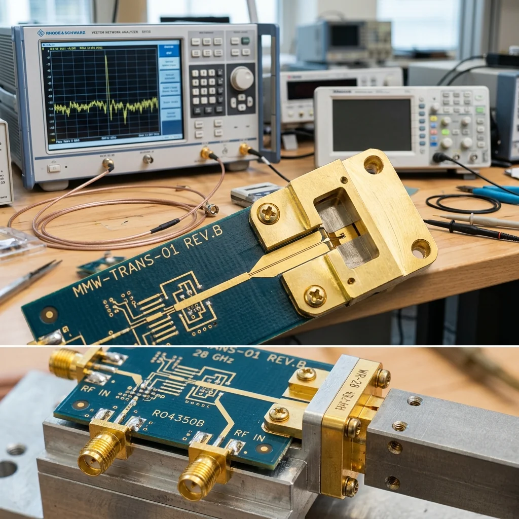
Every mmWave system that combines an MMIC with a waveguide antenna, filter, or test port requires a transition between the planar transmission line on the chip or PCB and the rectangular waveguide. This transition must transform the quasi-TEM mode of the microstrip into the TE₁₀ mode of the waveguide with minimal reflection and insertion loss across the operating bandwidth. At 77 GHz, where WR-10 waveguide dimensions are 2.54 mm by 1.27 mm, the transition geometry is measured in tenths of millimeters. A 50 μm positioning error can shift the return loss from 20 dB to 10 dB. Three transition architectures dominate practice: probe-coupled, slot-coupled, and antipodal fin-line.
Probe-Coupled Transitions
A probe-coupled transition inserts the end of a microstrip line into the waveguide through a hole in the broad wall. The microstrip conductor extends into the waveguide as a probe that excites the TE₁₀ mode. A backshort (a short-circuited waveguide section behind the probe) reflects energy forward, and the probe length and position are tuned to achieve impedance matching between the 50 Ω microstrip and the waveguide impedance (typically 400 to 500 Ω for standard rectangular waveguide).
The probe length is approximately λ_g/4 in the waveguide, where λ_g is the guide wavelength at the center frequency. The backshort distance from the probe is also approximately λ_g/4. These two quarter-wave sections create a resonant structure that provides excellent match at the design frequency. The bandwidth is determined by the Q-factor of the resonance: a higher Q gives a deeper match at center frequency but a narrower bandwidth.
Practical Considerations
- Substrate thickness: the probe penetration depth into the waveguide must be controlled to within ±25 μm. Substrate thickness tolerance directly affects probe position. Rogers 5880 (0.127 mm) and alumina (0.254 mm) are common substrates for Ka-band and above.
- Waveguide channel depth: the waveguide channel is typically machined into a metal block (split-block construction), and the PCB sits on top with the probe dropping into the channel. The channel depth tolerance must match the substrate stackup to within ±50 μm.
- Alignment pins: dowel pins align the PCB to the waveguide block. At W-band (75 to 110 GHz), pin diameter tolerance of ±10 μm is standard. Loose pins allow the probe to shift laterally, degrading return loss.
| Architecture | Bandwidth (typ.) | Insertion Loss | Return Loss | Frequency Range | Complexity |
|---|---|---|---|---|---|
| Probe-coupled | 15-25% | 0.3-0.8 dB | 15-25 dB | Up to 110 GHz | Medium |
| Slot-coupled | 10-20% | 0.5-1.2 dB | 15-20 dB | Up to 170 GHz | Low |
| Antipodal fin-line | 40-67% | 0.5-1.5 dB | 10-18 dB | Up to 220 GHz | High |
| Ridge probe | 25-40% | 0.4-1.0 dB | 15-22 dB | Up to 140 GHz | High |
Slot-Coupled Transitions
A slot-coupled transition places the microstrip substrate on the broad wall of the waveguide, with a resonant slot cut in the ground plane between the microstrip and the waveguide. The microstrip line crosses over the slot, and the slot couples electromagnetic energy from the microstrip's fringing fields into the waveguide's TE₁₀ mode. The slot dimensions (length approximately λ₀/2, width approximately λ₀/20) determine the coupling strength and center frequency.
The slot-coupled approach has a key mechanical advantage: the substrate does not penetrate the waveguide channel. The PCB sits flat on top of the waveguide flange surface, and only the slot in the ground plane provides the electromagnetic coupling. This simplifies assembly because there is no probe to align vertically within the waveguide. The trade-off is narrower bandwidth (typically 10 to 20% for a single resonant slot) and slightly higher insertion loss due to the indirect coupling mechanism.
Wideband Enhancement: A single resonant slot provides 10 to 15% bandwidth. Adding a second slot (dual-slot coupling) or replacing the simple slot with an H-shaped or bowtie-shaped aperture extends the bandwidth to 20 to 30%. These shaped apertures introduce additional resonances that broaden the impedance match at the cost of more complex PCB fabrication and tighter dimensional tolerances on the slot geometry.
Antipodal Fin-Line Transitions
An antipodal fin-line transition achieves the widest bandwidth of any microstrip-to-waveguide coupling method. The microstrip line gradually transforms into a pair of antipodal fins: two conductors on opposite sides of the substrate that taper from microstrip width to full waveguide height over a length of several guide wavelengths. The fins progressively fill the waveguide cross-section, smoothly converting the quasi-TEM microstrip mode into the TE₁₀ waveguide mode.
The transition bandwidth is determined by the taper length and profile. A linear taper achieves 40% bandwidth. A Klopfenstein or exponential taper profile extends bandwidth to 50 to 67% (full waveguide bandwidth). At W-band, a Klopfenstein fin-line transition can cover the entire 75 to 110 GHz range with return loss better than 15 dB across the band. This performance is unmatched by probe or slot designs.
The manufacturing challenge is substrate registration within the waveguide channel. The PCB must be centered in the waveguide cross-section to within ±25 μm in both the E-plane and H-plane directions. At 110 GHz (WR-10), the waveguide height is only 1.27 mm, and the substrate thickness (typically 0.127 mm or 0.254 mm) must sit precisely at the midplane. Split-block waveguide construction, where two machined halves clamp the substrate, is the standard approach. Five-axis CNC machining with ±5 μm tolerance produces the waveguide channels and alignment features.
Selecting the Right Architecture
- Narrowband systems (single channel, 10-15% BW): slot-coupled transition. Simplest assembly, lowest cost, adequate performance for single-frequency radar or communication links.
- Moderate bandwidth (15-25% BW): probe-coupled transition. Good balance of performance and manufacturability. The standard choice for Ka-band satellite terminals and 77 GHz automotive radar modules.
- Full waveguide bandwidth (40-67% BW): antipodal fin-line. Required for wideband instrumentation, multi-band systems, and test equipment that must cover an entire waveguide band.
- Above 110 GHz: fin-line transitions dominate because probe and slot dimensions become too small for reliable manufacturing. At 220 GHz (WR-3), the waveguide dimensions are 0.864 mm by 0.432 mm, and only photolithographic substrate patterning can achieve the required feature sizes.
RF Essentials supplies precision waveguide components that mate with microstrip transition assemblies, including calibration loads for characterizing transition performance using back-to-back measurements.
Flanged waveguide sections, terminations, and adapters for microstrip transition characterization. WR-10, WR-12, WR-15, and WR-28 in stock.