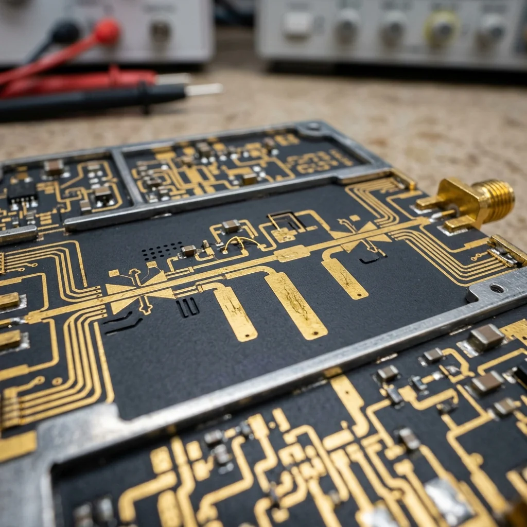
Impedance matching at Ka-band (26.5 to 40 GHz) demands a fundamentally different approach than matching at lower frequencies. Lumped components, the L-C networks that dominate matching below 6 GHz, become impractical. A 1 nH inductor at 30 GHz has a self-resonant frequency that may fall within the operating band. Parasitic capacitance from a chip capacitor's termination pads dominates its behavior above 20 GHz. At Ka-band, impedance matching is almost exclusively accomplished with distributed elements: sections of transmission line whose length and characteristic impedance are chosen to transform one impedance to another. The two primary tools are stub tuners and quarter-wave transformers, and selecting the right one depends on the impedance to be matched, the required bandwidth, and the physical constraints of the circuit.
Why Ka-Band Matching Is Different
At 30 GHz, a wavelength in free space is 10 mm. On a microstrip transmission line with an effective dielectric constant of 3.0, the guided wavelength drops to approximately 5.8 mm. A quarter wavelength is 1.45 mm. This is good news and bad news. The good news is that distributed matching elements are physically small, which allows compact circuit layouts. The bad news is that manufacturing tolerances that are negligible at lower frequencies become significant fractions of a wavelength at Ka-band.
A microstrip line etched on alumina (εr = 9.8) at 35 GHz has a guided wavelength of approximately 3.4 mm. A quarter-wave section is 0.85 mm long. If the fabrication process has a length tolerance of ±0.05 mm, that represents ±6% of the quarter-wave length, which translates directly to a phase error of ±21 degrees. This level of phase error can shift the match frequency by several GHz, potentially outside the intended operating band. The precision of the matching network at Ka-band is therefore limited by the precision of the manufacturing process.
| Matching Technique | Bandwidth (typical) | Design Complexity | Tunability | Best Application |
|---|---|---|---|---|
| Single stub | 5-10% | Low | Fixed (position + length) | Narrowband, known load |
| Double stub | 10-15% | Medium | Adjustable (length only) | Moderate BW, variable load |
| λ/4 transformer | 10-15% | Low | Fixed | Real impedance transformation |
| Multi-section λ/4 | 20-40% | Medium | Fixed | Broadband, real impedances |
| Tapered line | 30-50%+ | Low (design), high (fab) | Fixed | Ultra-broadband |
Stub Tuners: Maximum Flexibility
Single Stub Matching
A single stub matching network consists of a short- or open-circuited transmission line stub connected in shunt (parallel) or series with the main transmission line. The stub's susceptance (or reactance) cancels the reactive component of the load admittance (or impedance), while the position of the stub along the main line is chosen to present the correct conductance (or resistance) at the stub junction.
The design procedure on the Smith Chart is straightforward: rotate around the constant-VSWR circle from the load impedance until you reach the unity conductance circle (for shunt stubs). The rotation angle determines the stub position. The intersection with the unity conductance circle determines the required stub susceptance, which sets the stub length. At Ka-band, shunt open stubs are preferred because they avoid the difficulty of creating reliable RF short circuits at 30+ GHz. A radial stub provides a broadband open circuit at the stub's end.
Double Stub Matching
A double stub tuner uses two stubs at fixed positions along the line. The advantage is that the stub positions are predetermined (typically λ/8 or 3λ/8 apart), and only the stub lengths need to be adjusted to match any load impedance within the matchable region. This is particularly useful in waveguide laboratory setups where physical adjustable stub tuners (E-H tuners) allow real-time impedance matching during device characterization.
Design Tip: At Ka-band, always use electromagnetic simulation (HFSS, CST, or ADS Momentum) to verify stub matching networks. The simple transmission line model breaks down at millimeter-wave frequencies because of junction parasitics (the T-junction where the stub meets the main line introduces excess capacitance), radiation from open stubs, and surface wave excitation on thick substrates. A network that looks perfect in a circuit simulator may show 3 to 5 dB of return loss degradation when the full 3D geometry is simulated.
Quarter-Wave Transformers: Simplicity and Bandwidth
The quarter-wave transformer is the most elegant matching structure in microwave engineering. A section of transmission line with characteristic impedance Z₁ = √(Z₀ × Z_L) and length λ/4 transforms a real load impedance Z_L to the system impedance Z₀. No stubs, no junctions, no additional fabrication steps. Just a section of line with a different width.
At Ka-band on microstrip, changing the line width changes the characteristic impedance. A 50 Ω line on 10-mil alumina is approximately 0.24 mm wide. A 35 Ω line (for matching a 25 Ω load to 50 Ω) is approximately 0.55 mm wide. The step in width from 0.24 to 0.55 mm creates a discontinuity that adds parasitic capacitance. This capacitance must be compensated by shortening the transformer section or adding a small chamfer at the step.
Multi-Section Transformers for Broadband Matching
A single quarter-wave transformer has a bandwidth of approximately 10 to 15% for a 2:1 impedance ratio. For wider bandwidth, multiple quarter-wave sections are cascaded, each providing a smaller impedance step. The impedance values of the sections follow a taper function: binomial (maximally flat) or Chebyshev (equi-ripple).
A three-section Chebyshev transformer can match a 2:1 impedance ratio over a 30% bandwidth with better than 20 dB return loss. At Ka-band, a three-section design for matching 25 Ω to 50 Ω occupies approximately 3.5 mm on alumina, which is compact enough for most hybrid MIC and MMIC layouts. The WR-28 waveguide transitions that RF Essentials manufactures use multi-section transformer principles to achieve broadband impedance matching between rectangular waveguide and coaxial interfaces.
Waveguide Matching at Ka-Band
In waveguide systems, impedance matching uses different structures than microstrip. The waveguide equivalent of a stub tuner is an inductive or capacitive post, iris, or screw inserted into the waveguide cross-section. The waveguide equivalent of a quarter-wave transformer is a section of waveguide with modified dimensions (width, height, or both).
- Inductive posts: metal rods extending from the broad wall into the waveguide. They add shunt inductance and are used for narrowband matching. Adjustable versions (tuning screws) are common in waveguide filter assemblies and test setups.
- Capacitive irises: thin metal fins extending from the narrow walls. They add shunt capacitance. Used in filter and matching network design.
- Stepped impedance transformers: waveguide sections with reduced height (for impedance step-up) or increased width. Multi-step designs follow the same binomial/Chebyshev taper theory as microstrip transformers.
Selection Guidelines
- Load is purely real (or nearly real)? Use a quarter-wave transformer. It is the simplest solution with no additional elements.
- Load has significant reactive component? Use a single stub to cancel the reactance, optionally followed by a transformer for the remaining real mismatch.
- Bandwidth requirement exceeds 15%? Use a multi-section quarter-wave transformer (Chebyshev for equi-ripple) or a tapered line.
- Load impedance is unknown or variable? Use a double stub tuner in the lab, then replace with a fixed network once the load is characterized.
- Space-constrained MMIC layout? Prefer quarter-wave transformers over stubs. Stubs consume lateral space and radiate at open ends.
RF Essentials manufactures precision WR-28 waveguide components for Ka-band systems: transitions, adapters, bends, and calibration standards. All products maintain the dimensional tolerances required for matched impedance performance across the full 26.5 to 40 GHz band.